High-temperature Firing Pastes
CuAgTi-based
Conductor pastes(CuAgTi-based)
Product Details
Features
- By layering copper paste on the upper layer, it is possible to form an ultra-thick film of 0.3 mm or more.
- It does not contain environmentally hazardous substances such as Pb and Cd.
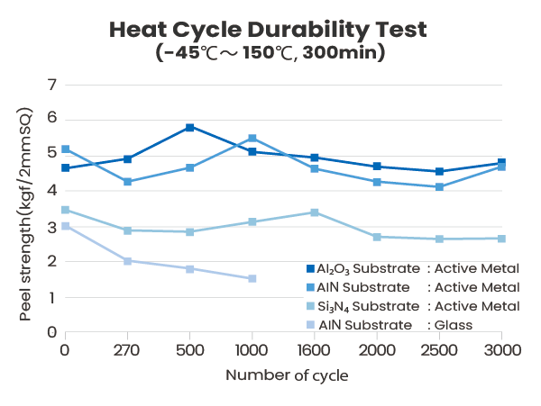
- It has excellent heat resistance, impact resistance, and reliability.
- The metal film and substrate form a strong chemical bond, providing excellent adhesion to Si₃N₄ and AlN substrates.
Structure
-

Film thickness of less than 100 μm
■Process
(1) Print the bonding layer (AS112)
(2) Print the upper layer of the bonding layer (DC014GL)
(3) Firing, e.g. 850℃, N₂ atmosphere -
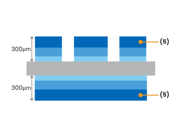
Film thickness of 100 μm or more
For a film thickness of 100 μm or more, the following process is added.
■Process
(4) Print the thickening layer (GL39)
(5) Firing, e.g. 800℃, N₂ atmosphere
-
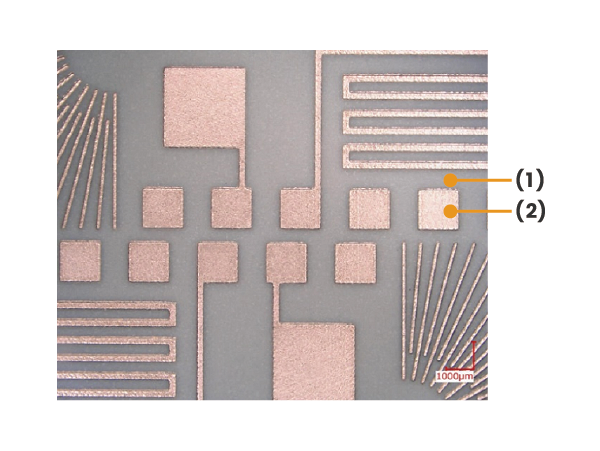
Substrate image after firing
Copper paste thick film (50μm) fired substrate using an active metal paste as the bonding layer.
(1) SiN
(2) Copper -
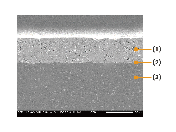
Cross-section SEM image
Substrate image after firing
(1) Copper film
(2) Active metal containing bonding layer (structural formula: Ti5Si3)
(3) SiN substrate
Application Example
-
- Ceramic heat dissipation circuit packages for power devices
- Ceramic circuit boards and ceramic packages that require high reliability
Specification
| Type | Film thickness | Application | Feature | Conductor component | Adhesive Strength (N/2mm□) | Recommended firing condition | Coating method | Substrate | |
|---|---|---|---|---|---|---|---|---|---|
| 100μm< | 100μm≧ | ||||||||
| AS112 | ○ | ○ | Thick film conductor wiring, Electrode formation (bonding layer with ceramic substrate) | High bonding strength, High thermal reliability | Ag, Cu, Ti |
≧30 |
850 °C 10min, |
Screen printing | Al₂O₃, AlN, Si₃N₄ |
| DC014GL | ○ | ○ | Thick film conductor wiring, Electrode formation | High surface smoothness, Larger film thickness can be formed in a single print | Cu | - | 850 °C 10min, In N₂ |
Screen printing | Al₂O₃, AlN, Si₃N₄ |
| GL39 | - | ○ | Ultra-thick film conductor wiring, Electrode formation(for multilayer thickening) | Larger film thickness can be formed in a single print | Cu | - | 800 °C 10min, In N₂ |
Screen printing | Al₂O₃, AlN, Si₃N₄ |
Caution
- It should be fired in a nitrogen atmosphere.
- Please check the Material Safety Data Sheet (SDS) for each product.
Remarks
If you do not have a replacement nitrogen furnace, we can fire it on your behalf.